| CPC H10K 59/131 (2023.02) [G06F 1/189 (2013.01)] | 21 Claims |

|
1. A display device comprising:
a substrate;
a TFT layer on the substrate, the TFT layer including a plurality of TFTs;
a plurality of light-emitting elements on the TFT layer, each of the plurality of light-emitting elements including a first electrode, a functional layer, and a second electrode; and
a sealing layer provided so as to cover the plurality of light-emitting elements,
the display device having: a display area where there are provided a plurality of pixels and a plurality of pixel circuits; and a frame area around the display area, wherein
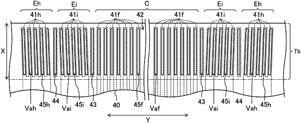
the frame area has an end portion including a first terminal portion including: a plurality of first signal terminal electrodes through which a signal is inputted to the plurality of pixel circuits; and a plurality of first power supply terminal electrodes through which a power supply voltage is inputted to the plurality of pixel circuits,
the display device further comprises a flexible printed board including a second terminal portion facing the first terminal portion,
the second terminal portion includes: a plurality of second signal terminal electrodes electrically connected to the plurality of first signal terminal electrodes via a conductive paste respectively; and a plurality of second power supply terminal electrodes electrically connected to the plurality of first power supply terminal electrodes via a conductive paste respectively,
the plurality of first signal terminal electrodes at least partially overlaps at least a part of the plurality of second signal terminal electrodes in a plan view, and the plurality of first power supply terminal electrodes at least partially overlaps at least a part of the plurality of second power supply terminal electrodes in a plan view, and
the plurality of first signal terminal electrodes and the plurality of second signal terminal electrodes are parallel to each other, and either the plurality of first power supply terminal electrodes or the plurality of second power supply terminal electrodes is inclined from the other.
|