| CPC H10K 59/131 (2023.02) [H10K 59/121 (2023.02)] | 20 Claims |

|
1. A display device comprising:
a display region formed with a notch portion; and
a frame region surrounding the display region,
wherein the display region includes
a plurality of data signal lines,
a plurality of control lines including a plurality of scanning control lines intersecting the plurality of data signal lines and a plurality of light emission control lines intersecting the plurality of data signal lines, and
a plurality of subpixel circuits corresponding to respective intersection points of the plurality of data signal lines and the plurality of scanning control lines,
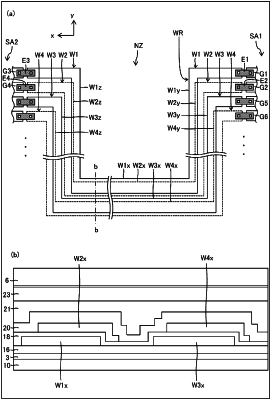
a first frame region on a periphery of the notch portion out of the frame region includes
a first lead wiring line electrically connected to a first control line and extending from the display region toward the notch portion, the first control line being one of the plurality of control lines, and
a second lead wiring line electrically connected to a second control line and extending from the display region toward the notch portion, the second control line being adjacent to the first control line,
in the display region, the first control line and the second control line are formed of a first metal layer,
in the first frame region on the periphery of the notch portion, the first lead wiring line is formed of the first metal layer, and the second lead wiring line is formed of a second metal layer, the second metal layer being a different layer from the first metal layer,
in a plan view, an extending direction of the first lead wiring line and an extending direction of the second lead wiring line are same,
the first lead wiring line and the second lead wiring line overlap each other via an inorganic insulating film, and
either one of the first lead wiring line and the second lead wiring line includes
a first region overlapping to straddle only an end portion of another one of the first lead wiring line and the second lead wiring line on a side opposite the display region in a direction orthogonal to the extending direction of the other lead wiring line, and
a second region overlapping to straddle only an end portion of the lead wiring line on a side closer to the display region in the direction orthogonal to the extending direction of the other lead wiring line.
|