| CPC H10K 59/131 (2023.02) [G09G 3/32 (2013.01); G09G 2300/0426 (2013.01); G09G 2310/0202 (2013.01); H10K 59/1201 (2023.02)] | 20 Claims |
|
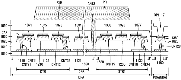
1. A display device comprising:
a substrate;
a first conductive layer disposed on the substrate, the first conductive layer including a data signal line and a capacitor lower electrode;
an interlayer insulating film disposed on the first conductive layer;
a semiconductor layer disposed on the interlayer insulating film, the semiconductor layer including a first semiconductor pattern;
a gate insulating film disposed on the semiconductor layer;
a second conductive layer disposed on the gate insulating film, the second conductive layer including:
a capacitor upper electrode overlapping the capacitor lower electrode;
a gate electrode of a first transistor disposed to overlap the first semiconductor pattern;
a first electrode of the first transistor disposed to overlap a part of the first semiconductor pattern, wherein the first electrode of the first transistor is electrically connected to the data signal line through a first contact hole that penetrates the interlayer insulating film and the gate insulating film; and
a second electrode of the first transistor disposed to overlap another part of the first semiconductor pattern; and
a third insulating layer disposed on the second conductive layer, wherein the gate electrode of the first transistor, the first electrode of the first transistor, the second electrode of the first transistor, and the capacitor upper electrode are disposed between the gate insulating film and the third insulating layer, and
a pixel electrode disposed on the third insulating layer, wherein
a second contact hole that penetrates the third insulating layer, the interlayer insulating film and the gate insulating film is defined to expose a portion of the capacitor lower electrode and
the pixel electrode is in direct contact with the portion of the capacitor lower electrode through the second contact hole.
|