| CPC H10K 59/124 (2023.02) [H10K 50/82 (2023.02); H10K 50/844 (2023.02); H10K 59/1213 (2023.02); H10K 71/221 (2023.02); H10K 71/621 (2023.02); H01L 27/1225 (2013.01); H01L 27/124 (2013.01); H10K 50/15 (2023.02); H10K 50/16 (2023.02); H10K 50/17 (2023.02); H10K 50/171 (2023.02); H10K 59/1201 (2023.02)] | 20 Claims |

|
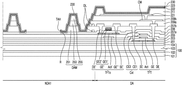
1. A method of manufacturing a display panel comprising a substrate that includes an opening area, a display area, and a non-display area, the display area surrounding the opening area, and the non-display area being between the opening area and the display area, the method comprising:
forming a pixel circuit on the display area of the substrate, the pixel circuit comprising at least one thin film transistor;
forming a sacrificial layer on an insulating layer located in the non-display area on the substrate;
forming a recess that is concave in a vicinity of the sacrificial layer in a depth direction of the insulating layer;
forming a first functional layer, a second functional layer, and an opposite electrode in the display area and the non-display area;
irradiating laser light of an infrared wavelength to a lower surface of the sacrificial layer from a lower surface of the substrate; and
forming a transmission hole in the first functional layer, the second functional layer, and the opposite electrode as the sacrificial layer irradiated with the laser light is lifted off from the insulating layer.
|