| CPC H10K 59/124 (2023.02) [H10K 50/84 (2023.02); H10K 59/122 (2023.02); H10K 59/123 (2023.02); H10K 59/131 (2023.02); H10K 71/00 (2023.02); H10K 2102/00 (2023.02)] | 21 Claims |
|
1. A display panel comprising:
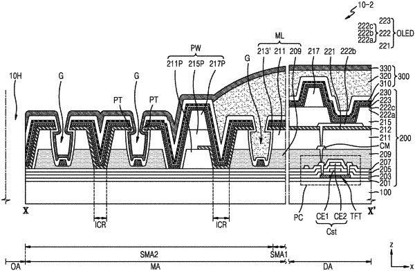
a substrate comprising a first area, a second area, and a third area between the first area and the second area;
a buffer layer on the substrate;
a transistor on the buffer layer, the transistor being located in the second area;
a stack structure in the second area, the stack structure comprising a pixel electrode electrically connected to the transistor, an opposite electrode, and an intermediate layer between the pixel electrode and the opposite electrode;
an encapsulation layer located on the stack structure and comprising at least one inorganic encapsulation layer and an organic encapsulation layer;
at least one partition wall in the third area; and
a plurality of grooves in the third area,
wherein the plurality of grooves comprise a first groove, and a bottom surface of the first groove is located above an upper surface of the buffer layer.
|