| CPC H10K 59/123 (2023.02) [H10K 50/818 (2023.02); H10K 59/124 (2023.02); H10K 71/00 (2023.02); H10K 50/813 (2023.02); H10K 59/35 (2023.02)] | 20 Claims |
|
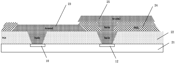
1. A display panel, comprising a plurality of first-color subpixels, wherein each first-color subpixel comprises:
a base, the base comprising a first driving electrode and a second driving electrode;
a flat layer disposed on a side, near the first driving electrode and the second driving electrode, of the base;
a patterned passivation layer and at least one first electrode disposed on the side, away from the base, of the flat layer, the first electrode being connected with the first driving electrode through via holes penetrating the flat layer; and
at least one second electrode disposed on the side, away from the base, of the patterned passivation layer, the second electrode being connected with the second driving electrode through via holes penetrating the patterned passivation layer and the flat layer.
|