| CPC H10K 59/121 (2023.02) [G09G 3/3233 (2013.01); H04N 23/53 (2023.01); H10K 59/1213 (2023.02); H10K 59/131 (2023.02); G09G 2300/0426 (2013.01); G09G 2300/0439 (2013.01); G09G 2300/0809 (2013.01); G09G 2320/0233 (2013.01)] | 11 Claims |
|
1. A light emitting device comprising a plurality of pixels arranged on a substrate in an array in a first direction and a second direction intersecting the first direction,
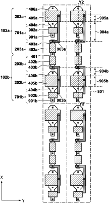
wherein each of the plurality of pixels includes (1) a light emitting element, (2) a first transistor having a first main terminal, of two main terminals of the first transistor, connected to an anode of the light emitting element, (3) a second transistor having a first main terminal, of two main terminals of the second transistor, connected to a gate electrode of the first transistor, and (4) a third transistor having a first main terminal, of two main terminals of the third transistor, connected to a second main terminal of the two main terminals of the first transistor,
wherein the plurality of pixels include a first pixel and a second pixel, which are adjacent to each other in the first direction,
wherein a second main terminal of the two main terminals of the second transistor of the first pixel and a second main terminal of the two main terminals of the second transistor of the second pixel share one diffusion region,
wherein the second main terminal, the gate electrode, and the first main terminal of the first transistor of the first pixel and the second main terminal, the gate electrode, and the first main terminal of the first transistor of the second pixel are sequentially arranged in one of a positive direction and a negative direction in the first direction, and
wherein a width of a wiring pattern between the gate electrode of the first transistor and the first main terminal of the second transistor of one of the first pixel and the second pixel is different from a width of a wiring pattern between the gate electrode of the first transistor and the first main terminal of the second transistor of another of the first pixel and the second pixel.
|