| CPC H10K 50/865 (2023.02) [H10K 50/8426 (2023.02); H10K 50/844 (2023.02); H10K 59/122 (2023.02); H10K 59/1315 (2023.02); H10K 59/38 (2023.02); H10K 59/40 (2023.02)] | 9 Claims |
|
1. A display device comprising:
a first substrate including a display area and a peripheral area outside the display area;
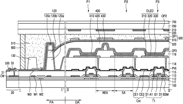
a plurality of organic light-emitting diodes in the display area, each of the plurality of organic light-emitting diodes including a pixel electrode, an intermediate layer, and an opposite electrode;
a thin-film encapsulation layer covering the plurality of organic light- emitting diodes and including a first inorganic encapsulation layer, an organic encapsulation layer, and a second inorganic encapsulation layer that are sequentially stacked;
a buffer layer arranged on the thin-film encapsulation layer and covering the display area and the peripheral area;
a pattern layer on the buffer layer, the pattern layer including a first light- blocking pattern shielding a portion of an area between two adjacent organic light-emitting diodes of the plurality of organic light-emitting diodes and
a terminal arranged in the peripheral area and a connection wiring arranged below the terminal, wherein the buffer layer directly contacts a portion of the terminal, and the buffer layer includes
a first contact hole that exposes the terminal and a width of the terminal is greater than a width of the connection wiring.
|