| CPC H10K 50/844 (2023.02) [H10K 59/12 (2023.02); H10K 77/111 (2023.02)] | 12 Claims |
|
1. A display panel comprising:
a flexible substrate;
a plurality of self-luminescent elements provided on a first main face of the flexible substrate;
a plurality of thin film transistor (TFT) circuits provided between the first main face and the plurality of self-luminescent elements and driving the self-luminescent elements;
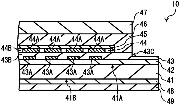
a first inorganic film provided between the plurality of TFT circuits and the plurality of self-luminescent elements, covering the TFT circuits, and having a step portion, the step portion being a thinned portion of the first inorganic film opposed to an end portion of the flexible substrate;
a second inorganic film covering the self-luminescent elements; and
a resin layer covering the second inorganic film and covering at least a portion of the first inorganic film in contact with an end portion of the second inorganic film.
|