| CPC H10K 50/844 (2023.02) [H10K 50/16 (2023.02); H10K 50/171 (2023.02); H10K 71/00 (2023.02)] | 18 Claims |
|
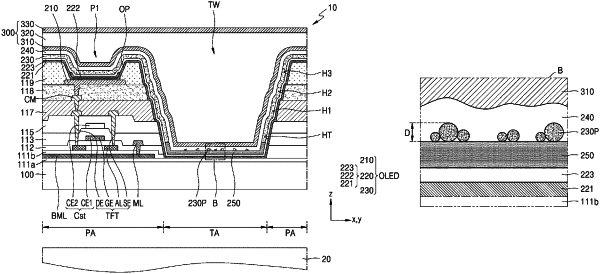
1. A display apparatus comprising:
a substrate including:
a display area including a transmission area and a pixel area; and
a peripheral area adjacent to the display area;
a display element disposed corresponding to the pixel area, the display element comprising:
a pixel electrode;
an intermediate layer on the pixel electrode; and
an opposite electrode on the intermediate layer;
a hydrophobic layer disposed corresponding to the transmission area; and
a plurality of fine particles disposed directly on a top surface of the hydrophobic layer, the plurality of fine particles and the opposite electrode comprising a same material.
|