| CPC H10K 50/813 (2023.02) [H10K 50/865 (2023.02); H10K 71/00 (2023.02); H10K 2102/102 (2023.02); H10K 2102/103 (2023.02)] | 4 Claims |
|
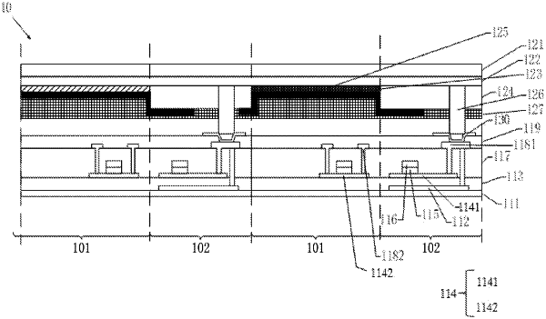
1. A display panel, comprising a light-emitting region and a non-light-emitting region surrounding the light-emitting region;
a first substrate, wherein a first leading line is disposed on one side of the first substrate; and
a second substrate connected to the side of the first substrate comprising the leading line;
wherein the second substrate comprises a cover plate;
a first electrode disposed on one side of the cover plate in a direction of the first substrate, and extending from the non-light-emitting region to the light-emitting region;
a retaining wall structure disposed on the first electrode, wherein the retaining wall structure comprises a plurality of through-holes and a plurality of retaining walls surrounding the through-holes, and the retaining walls are disposed in the non-light-emitting region;
a light-emitting layer comprising a plurality of light-emitting units, wherein any one of the light-emitting units is correspondingly disposed in the through-holes of the retaining wall structure;
a second electrode disposed on the light-emitting layer and extending to cover a portion of the retaining wall structure adjacent to the second electrode;
a packaging layer disposed on the first electrode and covering the retaining wall structure, the light-emitting layer, and the second electrode; and
a second leading line disposed on the first electrode of the non-light-emitting region, wherein the second leading line penetrates through the retaining wall structure and the packaging layer;
wherein the first substrate comprises:
a base substrate;
a light-shielding metal layer disposed in the non-light-emitting region on the base substrate;
a buffer layer disposed on the second substrate and covering the light-shielding metal layer;
an active layer disposed on the buffer layer;
a first insulating layer disposed on the active layer, wherein an orthographic projection of the first insulating layer on the base substrate completely falls within an orthographic projection of the active layer on the base substrate;
a first metal layer disposed on the first insulating layer; and
a second insulating layer disposed on the buffer layer and covering the active layer, the first insulating layer, and the first metal layer;
wherein the active layer comprises:
a first active layer disposed in the non-light-emitting region and corresponding to the light-shielding metal layer;
a second active layer disposed in the light-emitting region;
a second metal layer disposed on the second insulating layer and comprising a first metal segment disposed in the non-light-emitting region and corresponding to the first active layer, wherein the first metal segment comprises at least two pins, one of the pins penetrates through the second insulating layer to connect to the first active layer, and another pin penetrates through the second insulating layer and the buffer layer to connect to the light-shielding metal layer; and
a third insulating layer disposed on the second insulating layer and covering the second metal layer, wherein a via hole is defined in the third insulating layer corresponding to the first metal segment, the first leading line is disposed on an inner surface of the via hole and covers a region where the first metal segment is exposed from the via hole, and the first leading line is connected to the first metal segment.
|