| CPC H10K 50/17 (2023.02) [H10K 50/156 (2023.02); H10K 71/00 (2023.02); H10K 2102/00 (2023.02); H10K 2102/351 (2023.02)] | 8 Claims |
|
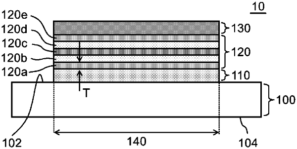
1. A light emitting device comprising:
a first electrode;
an organic layer positioned over the first electrode and comprising a first layer; and
a second electrode positioned over the organic layer,
wherein the first layer comprises
a first region comprising a first organic material and a compound comprising a metal element, the first region being in contact with the first electrode,
a second region comprising the first organic material and the compound, the second region being positioned farther away from the first electrode than the first region, and
a third region comprising the first organic material and the compound, the third region being positioned between the first region and the second region,
an average intensity of a SIMS profile of the metal element in the second region is lower than 10% of an average intensity of a SIMS profile of the metal element in the first region,
an intensity distribution of the SIMS profile of the metal element in the first region and an intensity distribution of the SIMS profile of the metal element in the second region are more uniform than an intensity distribution of a SIMS profile of the metal element in the third region, and
an intensity of the SIMS profile of the metal element in the third region decreases from the first region to the second region.
|