| CPC H10K 30/82 (2023.02) [H01L 27/14665 (2013.01); H01L 31/0224 (2013.01); H01L 31/035209 (2013.01); H10K 30/81 (2023.02); H01L 31/022466 (2013.01); H01L 31/022475 (2013.01); H01L 2924/0134 (2013.01); H10K 39/32 (2023.02)] | 10 Claims |
|
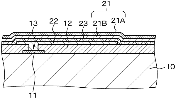
1. An electronic device, comprising:
a first electrode, a second electrode and a photoelectric conversion layer disposed between the first electrode and the second electrode,
the first electrode including an amorphous oxide including one or both of a quaternary compound of indium, zinc, gallium and oxygen and a quaternary compound of indium, zinc, aluminum and oxygen,
wherein the first electrode has a laminated structure including a first B layer and a first A layer from a photoelectric conversion layer side, and a work function value of the first A layer of the first electrode being lower than a work function value of the first B layer of the first electrode.
|