| CPC H10K 19/10 (2023.02) [H01L 21/822 (2013.01); H01L 27/0688 (2013.01); H01L 28/10 (2013.01); H01L 28/40 (2013.01); H10K 19/201 (2023.02)] | 20 Claims |
|
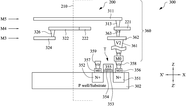
1. An integrated circuit (IC) device, comprising:
a substrate; and
a circuit region over the substrate, the circuit region comprising:
at least one active region extending along a first direction;
at least one gate region extending across the at least one active region and along a second direction transverse to the first direction; and
at least one first input/output (IO) pattern configured to electrically couple the circuit region to external circuitry outside the circuit region,
wherein
the at least one first IO pattern extends along a third direction oblique to both the first direction and the second direction,
the circuit region has a boundary, and
the at least one first IO pattern is completely arranged within the boundary of the circuit region.
|