| CPC H10B 99/00 (2023.02) [H01L 21/76802 (2013.01); H01L 21/76877 (2013.01)] | 16 Claims |
|
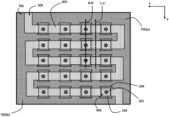
1. A method for manufacturing a 3D vertical array of memory cells, comprising:
forming, on a substrate, a stack of dielectric material layers comprising alternating first and second dielectric material layers;
forming a trench through the stack of dielectric material layers, the trench exposing the substrate;
filling the trench with a third dielectric material;
forming holes through the stack of dielectric material layers, the holes exposing the substrate, wherein forming the holes through the stack of dielectric material layers comprises forming the holes in the third dielectric material filling the trench;
selectively removing the second dielectric material layers through the holes to form cavities between adjacent first dielectric material layers;
filling the cavities with a conductive material through the holes to form corresponding conductive material layers;
forming first memory cell access lines from the conductive material layers;
carrying out a conformal deposition of a chalcogenide material through the holes;
forming memory cell storage elements from the deposited chalcogenide material; and
filling the holes with conductive material to form corresponding second memory cell access lines.
|