| CPC H10B 63/34 (2023.02) [H10B 41/00 (2023.02); H10B 61/22 (2023.02); H10B 63/32 (2023.02); H10B 63/84 (2023.02)] | 17 Claims |
|
1. A method of selectively operating a semiconductor device as a memory select transistor with increased on-state drain current, said method comprising:
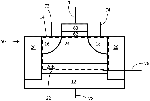
providing said semiconductor device comprising a substrate having a first conductivity type selected from p-type conductivity type and n-type conductivity type; a buried layer having a second conductivity type selected from said p-type conductivity type and said n-type conductivity type and being different from said first conductivity type; a body having said first conductivity type; a source region and a drain region each having said second conductivity type and being separated by said body; and a gate positioned in between said source region and said drain region; wherein said semiconductor device is configured to function as a select transistor for at least one memory element connected to said drain region or said source region, wherein a state of said at least one memory element is determined by a resistivity of said at least one memory element; and
selectively operating said semiconductor device as said semiconductor memory device or said transistor, wherein said selectively operating comprises:
applying a relatively low voltage to said buried layer to operate said semiconductor device as said memory select transistor wherein said memory select transistor operates as an ordinary memory select transistor with a first amount of on-state drain current;
applying a relatively high voltage to said buried layer to operate said semiconductor device as said semiconductor memory device, wherein said semiconductor memory device has at least two stable states; and
applying an intermediate high voltage higher than said relatively low voltage but lower than said relatively high voltage to said buried layer to operate said semiconductor device as said memory select transistor with increased on-state drain current, relative to said first amount of on-state drain current.
|