| CPC H10B 61/22 (2023.02) [H10N 50/01 (2023.02); H10N 50/80 (2023.02)] | 20 Claims |
|
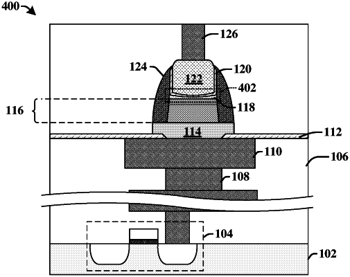
1. An integrated chip, comprising:
one or more lower interconnect layers arranged within one or more stacked inter-level dielectric (ILD) layers over a substrate;
an etch stop structure disposed over the one or more lower interconnect layers;
a bottom electrode disposed over the etch stop structure, wherein the bottom electrode electrically contacts the one or more lower interconnect layers;
a magnetic tunnel junction (MTJ) stack disposed over the bottom electrode, wherein the MTJ stack has sidewalls arranged at a first angle with respect to a bottom surface of the MTJ stack;
a top electrode disposed over the MTJ stack, wherein the top electrode has sidewalls arranged at a second angle with respect to a bottom surface of the top electrode, the second angle greater than the first angle; and
a diffusion barrier layer continuously extending from between the top electrode and the MTJ stack to along the sidewalls of the top electrode, wherein the diffusion barrier layer has a curved upper surface that increases in height as a distance from the sidewalls of the top electrode decreases.
|