| CPC H10B 53/30 (2023.02) [G11C 11/221 (2013.01); G11C 11/2259 (2013.01); G11C 11/2275 (2013.01); H01L 21/02565 (2013.01); H01L 29/66969 (2013.01); H01L 29/7869 (2013.01)] | 20 Claims |
|
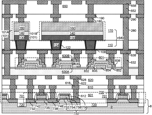
1. A memory device comprising:
metal interconnect structures embedded within dielectric material layers that overlie a top surface of a substrate;
a thin film transistor embedded in a first dielectric material layer selected from the dielectric material layers, and is vertically spaced from the top surface of the substrate; and
a ferroelectric memory cell embedded within the dielectric material layers,
wherein a first node of the ferroelectric memory cell is electrically connected to a node of the thin film transistor through a subset of the metal interconnect structures that is located above, and vertically spaced from, the top surface of the substrate, wherein the ferroelectric memory cell is located at a same level as the thin film transistor and is laterally surrounded by the first dielectric material layer.
|