| CPC H10B 43/35 (2023.02) [G11C 5/063 (2013.01); H10B 43/10 (2023.02)] | 17 Claims |
|
1. A method for manufacturing a non-volatile memory device, the method comprising:
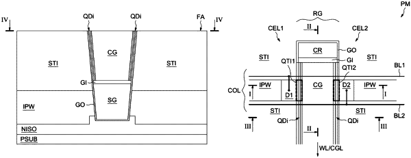
forming a trench extending vertically in a semiconductor well of a semiconductor substrate;
forming a source region at a bottom of the trench;
forming a gate dielectric layer around sidewalls of the trench;
forming, in the trench, a selection gate, the gate dielectric layer disposed between the semiconductor well and the selection gate;
forming a dielectric area on the sidewalls of the trench above the selection gate, the dielectric area comprising two charge trapping dielectric interfaces; and
forming, above the selection gate in the trench, a control gate, the control gate being laterally surrounded by the two charge trapping dielectric interfaces.
|