| CPC H10B 43/27 (2023.02) [G11C 13/0004 (2013.01); G11C 13/0069 (2013.01); G11C 16/0483 (2013.01); G11C 16/10 (2013.01); H10B 41/27 (2023.02); H10B 63/34 (2023.02); H10B 63/845 (2023.02); H10N 70/231 (2023.02); G11C 2213/75 (2013.01)] | 2 Claims |
|
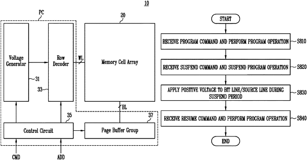
1. A method of operating a semiconductor memory device, the method comprising:
performing a program operation on a plurality of memory cells each including a channel layer, a tunnel insulating layer, an emission preventing layer, a charge storage layer, a blocking insulating layer, and a compensation charge storage layer in response to a program command;
suspending the program operation in response to a suspend command received from outside of the semiconductor memory device, and applying a positive voltage to bit lines or a source line, connected to the memory cells, during a suspend period; and
re-performing the suspended program operation in response to a resume command received from outside of the semiconductor memory device.
|