| CPC H10B 43/27 (2023.02) [H01L 29/40114 (2019.08); H01L 29/40117 (2019.08); H10B 41/27 (2023.02); H10B 41/35 (2023.02); H10B 43/35 (2023.02)] | 20 Claims |
|
1. A method for forming a channel hole plug structure in a three-dimensional (3D) memory device, comprising:
forming an alternating dielectric stack disposed on a substrate;
forming an insulating layer and a hard mask layer on the alternating dielectric stack;
forming a channel structure, comprising:
forming a channel hole penetrating the insulating layer, the hard mask layer, and the alternating dielectric stack;
forming a functional layer on a sidewall of the channel hole; and
forming a channel layer covering at least a portion of the functional layer on the sidewall of the channel hole and in direct contact with a top surface of the hard mask layer;
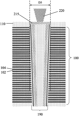
removing a top portion of the channel structure and a portion of the insulating layer surrounding the top portion of the channel structure to form a recess; and
forming a channel hole plug in the recess, wherein a projection of the channel hole plug in a lateral plane covers a projection of the channel structure in the lateral plane.
|