| CPC H10B 43/27 (2023.02) [H10B 41/27 (2023.02)] | 6 Claims |
|
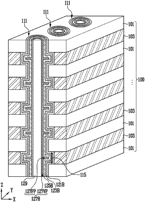
1. A semiconductor memory device, comprising:
a stacked body including interlayer insulating layers and word lines that are alternately stacked;
a hole passing through the stacked body, wherein sidewalls of the interlayer insulating layers are disposed farther from a central axis of the hole than sidewalls of the word lines to define a recess area between the word lines;
a channel layer formed in the hole;
a blocking insulating layer between each of the word lines and the channel layer;
a data storage layer between the blocking insulating layer and the channel layer; and
a tunnel insulating layer between the channel layer and the data storage layer,
wherein the tunnel insulating layer extends to fill a central portion of the recess area,
wherein the tunnel insulating layer includes Metal Organic Frameworks (MOF) having a lower dielectric constant than a dielectric constant of the blocking insulating layer.
|