| CPC H10B 43/27 (2023.02) [G11C 7/18 (2013.01); G11C 8/14 (2013.01); H01L 25/065 (2013.01); H10B 43/10 (2023.02)] | 20 Claims |
|
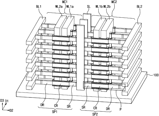
1. A semiconductor memory device comprising:
a plurality of first conductive lines stacked in a first direction perpendicular to a top surface of a substrate and extending lengthwise in a second direction parallel to the top surface of the substrate;
a plurality of second conductive lines extending lengthwise in the first direction and spaced apart from the plurality of first conductive lines in a third direction parallel to the top surface of the substrate and different from the second direction; and
a plurality of memory cells, each being provided at a corresponding one of a plurality of intersection points between the plurality of first conductive lines and the plurality of second conductive lines,
wherein each of the plurality of memory cells comprises a semiconductor pattern extending parallel to the top surface of the substrate, the semiconductor pattern including a source region having a first conductivity type, a drain region having a second conductivity type different from the first conductivity type, and a channel region between the source region and the drain region;
first and second gate electrodes surrounding the channel region of the semiconductor pattern; and
a charge storage pattern between the semiconductor pattern and each of the first and second gate electrodes,
wherein the first gate electrode is between the source region and the drain region and the second gate electrode is between the first gate electrode and the drain region, in each of the plurality of memory cells.
|