| CPC H10B 43/27 (2023.02) [H01L 29/40117 (2019.08); H01L 29/4234 (2013.01); H01L 29/512 (2013.01); H10B 43/35 (2023.02)] | 20 Claims |
|
1. A method of forming a memory device, the method comprising:
forming a layered structure above a conductive region, with the layered structure having a vertical opening bounded by a sidewall;
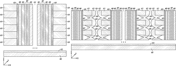
forming, on and contacting the sidewall, material for dielectric barriers for a vertical arrangement of multiple charge trap structures, the material for dielectric barriers structured as a nanolaminate of multiple regions of different material compositions, with each charge trap structure having a charge trap region separated from a portion of the material for dielectric barriers by a dielectric blocking region; and
forming gates of the multiple charge trap structures, with the gates of adjacent charge trap structures separated by a void, each void having the material for dielectric barriers as a portion of a boundary of the void, with the material for dielectric barriers continuously extending vertically between and as a part of the multiple charge trap structures in the formed memory device.
|