| CPC H10B 43/27 (2023.02) [H01L 21/0214 (2013.01); H01L 21/02164 (2013.01); H01L 21/02636 (2013.01); H01L 21/30604 (2013.01); H01L 21/31116 (2013.01); H01L 21/7682 (2013.01); H01L 29/40117 (2019.08)] | 20 Claims |
|
1. A three-dimensional (3D) memory device, comprising:
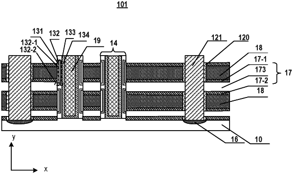
a stack structure on a substrate, the stack structure comprising a plurality of conductor layers each insulated from one another by a first composite layer, a second composite layer, and an airgap, wherein the first composite layer completely covers an entire bottom surface of an upper one of two adjacent conductor layers, the second composite layer completely covers an entire top surface of a lower one of two adjacent conductor layers, the first composite layer and the second composite layer of the two adjacent conductor layers are fully and completely separated by the airgap extending along a lateral direction, each of the first and second composite layers comprises a sub-layer of silicon oxynitride between a pair of sub-layers of silicon oxide extending along the lateral direction; and
a channel structure extending from a top surface of the stack structure to the substrate along a vertical direction, wherein the channel structure comprises:
a memory layer between a blocking layer and a tunneling layer, the memory layer comprising a plurality of memory layer segments each being disconnected from one another and corresponding to a respective one of conductor layers, wherein each of the memory layer segments comprises a vertical portion along the vertical direction and at least one lateral portion along the lateral direction, wherein the memory layer, the blocking layer, and the tunneling layer are partially exposed by the airgap; and
a source structure extending from the top surface of the stack structure to the substrate, wherein the source structure comprises a source contact and an insulating structure, and both the source contact and the insulating structure are partially exposed by the airgap.
|