| CPC H10B 41/44 (2023.02) [H01L 21/0276 (2013.01); H01L 21/28035 (2013.01); H01L 21/31053 (2013.01); H01L 21/31111 (2013.01); H01L 21/3212 (2013.01); H01L 21/32133 (2013.01); H01L 21/32139 (2013.01); H01L 21/76224 (2013.01); H01L 21/76802 (2013.01); H01L 29/0847 (2013.01); H01L 29/40114 (2019.08); H01L 29/42328 (2013.01); H01L 29/4916 (2013.01); H01L 29/66545 (2013.01); H01L 29/6656 (2013.01); H01L 29/66825 (2013.01); H01L 29/788 (2013.01); H10B 41/30 (2023.02)] | 20 Claims |

|
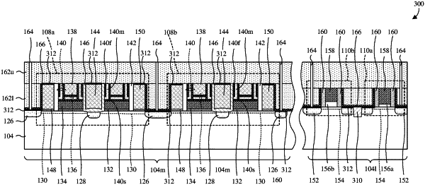
1. An integrated circuit (IC) comprising:
a memory region and a logic region integrated in a substrate;
a plurality of memory cell structures disposed on the memory region, each memory cell structure of the plurality of memory cell structures comprising a control gate electrode disposed over the substrate, a select gate electrode disposed on one side of the control gate electrode, and a spacer between the control gate electrode and the select gate electrode;
a contact etch stop layer (CESL) disposed along an upper surface of the substrate, extending upwardly along the select gate electrode within the memory region; and
a lower inter-layer dielectric layer disposed on the CESL and fill between the plurality of memory cell structures within the memory region,
wherein the CESL is in direct contact with sidewalls of the select gate electrode and the lower inter-layer dielectric layer.
|