| CPC H10B 41/42 (2023.02) [H01L 29/40114 (2019.08); H01L 29/40117 (2019.08); H01L 29/42328 (2013.01); H01L 29/42344 (2013.01); H01L 29/66795 (2013.01); H01L 29/66825 (2013.01); H01L 29/66833 (2013.01); H01L 29/7851 (2013.01); H01L 29/7881 (2013.01); H01L 29/792 (2013.01); H10B 43/40 (2023.02)] | 18 Claims |
|
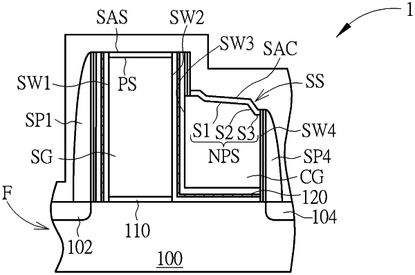
1. A semiconductor memory device, comprising:
a semiconductor substrate;
a select gate disposed on the semiconductor substrate, wherein the select gate comprises a first sidewall and a second sidewall opposite to the first sidewall;
a control gate disposed on the semiconductor substrate and in proximity to the second sidewall of the select gate, wherein the control gate comprises a third sidewall in proximity to the second sidewall, a fourth sidewall opposite to the third sidewall, and a non-planar top surface between the third sidewall and the fourth sidewall, wherein the non-planar top surface descending from the third sidewall to the fourth sidewall, wherein the first surface region, wherein the non-planar top surface comprises a first surface region between the third sidewall and the fourth sidewall and a second surface region between the first surface and the fourth sidewall, and wherein a slope of the second surface region is greater than that of the first surface region, and wherein the first surface region and the second surface region are covered with a metal silicide layer; and
a charge storage layer disposed between the control gate and the semiconductor substrate, wherein the charge storage layer extends onto the second sidewall, wherein the charge storage layer covers an entire surface of the second sidewall and protrudes from a top surface of the metal silicide layer, and wherein an outer surface of the charge storage layer above the control gate is covered with a spacer, wherein the spacer does not extend onto a top surface of the charge storage layer, wherein the metal silicide layer is disposed on the non-planar top surface not covered by the spacer.
|