| CPC H10B 41/27 (2023.02) [G11C 16/0483 (2013.01); G11C 16/10 (2013.01); H01L 21/76885 (2013.01); H01L 23/528 (2013.01); H01L 29/7889 (2013.01); H10B 41/30 (2023.02)] | 11 Claims |
|
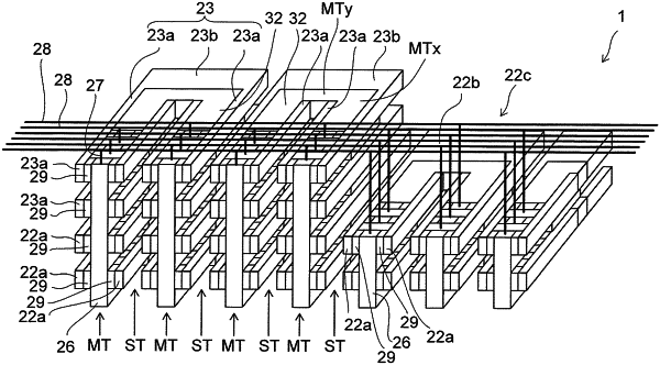
1. A semiconductor memory device, comprising:
a substrate;
a first wiring provided above the substrate and extending in a first direction parallel to a surface of the substrate;
a second wiring provided above the substrate and extending in the first direction, the first wiring and the second wiring being arranged at a second direction parallel to the surface of the substrate, the second direction crossing the first direction;
a first semiconductor pillar extending in a third direction away from the substrate;
a second semiconductor pillar extending in the third direction, the first semiconductor pillar and the second semiconductor pillar being arranged at the second direction;
a first memory cell provided on a side surface of the first semiconductor pillar, the first memory cell being provided between the first semiconductor pillar and the first wiring in the second direction, and the first memory cell being controllable by the first wiring;
a second memory cell provided on another side surface of the first semiconductor pillar, the second memory cell facing the first memory cell via the first semiconductor pillar in the second direction, the second memory cell being controllable by the second wiring;
a third memory cell provided on a side surface of the second semiconductor pillar, the third memory cell being controllable by applying a voltage to a first signal line electrically connected to the second wiring;
a first insulating layer being in contact with a first end portion of the second wiring in the first direction;
a third wiring provided above the substrate and extending in the first direction, the second wiring and the third wiring being arranged at the second direction;
a fourth memory cell provided on another side surface of the second semiconductor pillar, the fourth memory cell facing the third memory cell via the second semiconductor pillar in the second direction, the fourth memory cell being controllable by the third wiring; and
a second insulating layer being in contact with a second end portion of the third wiring in the first direction, the second insulating layer being provided at a different location away from the first insulating layer in the first direction and the second direction.
|