| CPC H10B 41/27 (2023.02) [H01L 23/5283 (2013.01); H10B 41/10 (2023.02); H10B 41/35 (2023.02); H10B 41/40 (2023.02); H10B 43/10 (2023.02); H10B 43/27 (2023.02); H10B 43/35 (2023.02); H10B 43/40 (2023.02)] | 18 Claims |
|
1. A semiconductor device comprising:
a stack structure comprising a plurality of mold layers and a plurality of horizontal conductive layers, which are alternately stacked;
a channel structure vertically extending in the stack structure;
a pillar structure vertically extending in the stack structure; and
a plurality of contact plugs, each being connected to a corresponding one of the plurality of horizontal conductive layers,
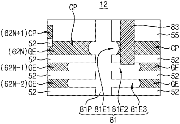
wherein each of the plurality of horizontal conductive layers comprises a gate electrode, and a connecting pad in continuity with the gate electrode,
wherein the pillar structure comprises a pillar extending through the plurality of horizontal conductive layers, and a plurality of pillar extensions protruding from a side surface of the pillar,
wherein the plurality of the pillar extensions comprise an uppermost extension and other pillar extensions,
wherein outer side surfaces of the other pillar extensions further protrude beyond an outer side surface of the uppermost pillar extension,
wherein each of the plurality of pillar extensions is horizontally aligned with a corresponding one of the plurality of horizontal conductive layers,
wherein the channel structure vertically extends through a plurality of gate electrodes of the plurality of horizontal conductive layers, and
wherein each of the plurality of contact plugs contacts a connecting pad of a corresponding one of the plurality of horizontal conductive layers.
|