| CPC H10B 12/485 (2023.02) [H10B 12/033 (2023.02); H10B 12/053 (2023.02); H10B 12/315 (2023.02); H10B 12/34 (2023.02); H10B 12/482 (2023.02)] | 12 Claims |
|
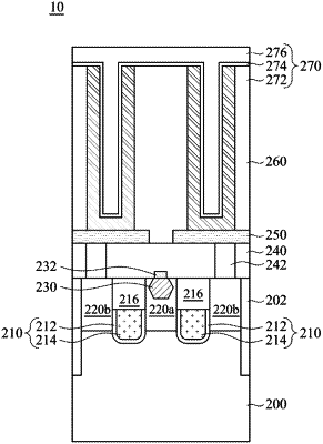
1. A method of manufacturing a memory structure, comprising:
forming a first gate structure, a second gate structure, and a plurality of source/drain regions in a substrate, wherein the plurality of source/drain regions are disposed on opposite sides of the first gate structure and the second gate structures;
performing a dry etching process to form a trench between the first gate structure and the second gate structure;
performing a wet etching process to expand the trench to form an expanded trench, wherein the expanded trench has a hexagonal shaped cross section; and
forming a bit line contact in the expanded trench.
|