| CPC H10B 12/34 (2023.02) [H10B 12/053 (2023.02)] | 15 Claims |

|
1. A method of manufacturing a semiconductor structure, comprising:
providing a substrate, and forming a trench extending downward in the substrate;
forming a gate dielectric layer on sidewalls and a bottom surface of the trench;
forming a barrier layer on a lower portion of sidewalls and a bottom surface of the gate dielectric layer;
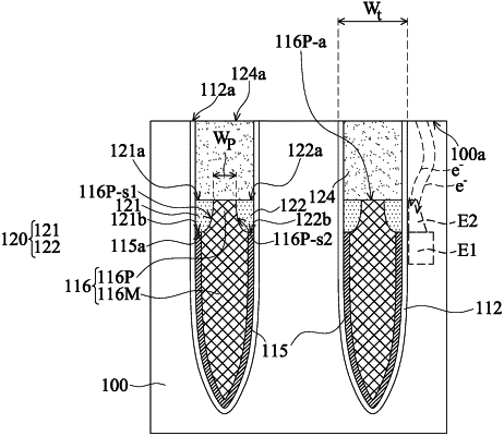
forming a first work function layer on a lower portion of the trench, wherein the first work function layer comprises:
a main portion in the lower portion of the trench, wherein the barrier layer surrounds sidewalls and a bottom surface of the main portion; and
a protruding portion on the main portion and connecting the main portion, wherein an area of a top surface of the protruding portion is less than an area of a bottom surface of the protruding portion;
forming a second work function layer at opposite sides of the protruding portion of the first work function layer; and
forming an insulating layer on the protruding portion of the first work function layer and on the second work function layer,
wherein forming the barrier layer and forming the first work function layer comprise:
forming a barrier material layer on the gate dielectric layer;
forming a first work function material layer on the barrier material layer;
recessing the first work function material layer to form a recessed first work function material layer;
forming a mask on the recessed first work function material layer, wherein the mask exposes a portion of a top surface of the recessed first work function material layer;
performing an etching step by using the mask to remove the portion of the recessed first work function material layer that is not covered by the mask, thereby forming the first work function layer.
|