| CPC H10B 12/34 (2023.02) [H01L 21/28088 (2013.01); H01L 21/28176 (2013.01); H01L 21/28194 (2013.01); H01L 21/32136 (2013.01); H01L 21/32155 (2013.01); H01L 21/76224 (2013.01); H01L 29/4236 (2013.01); H01L 29/4966 (2013.01); H01L 29/4983 (2013.01); H01L 29/513 (2013.01); H01L 29/518 (2013.01); H01L 29/66795 (2013.01); H01L 29/785 (2013.01); H10B 12/053 (2023.02); H10B 12/056 (2023.02); H10B 12/36 (2023.02); H01L 21/31053 (2013.01); H01L 29/517 (2013.01)] | 8 Claims |
|
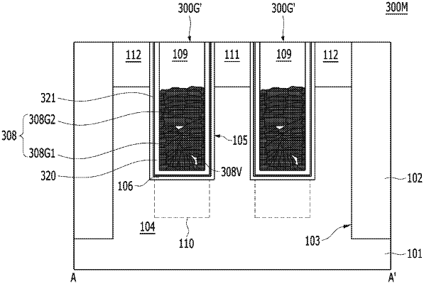
1. A semiconductor device, comprising:
a gate trench that is extended into a semiconductor substrate;
a gate dielectric layer formed in the gate trench to cover an inside surface of the gate trench;
a crystallization delay layer disposed over the gate dielectric layer;
a gate electrode disposed over the crystallization delay layer to fill a lower part of the gate trench; and
an interface layer disposed between the crystallization delay layer and the gate dielectric layer;
wherein the gate electrode includes first crystal grains and second crystal grains in a columnar structure;
wherein the first crystal grains are free of voids at an interface between the gate electrode and the crystallization delay layer formed by a crystal grain growth of an amorphous material,
wherein the second crystal grains are formed by a crystal grain growth of a polycrystalline material, and wherein said crystal growth includes annealing the amorphous and the polycrystalline materials at a temperature of from 300 *C to 1100 *C; and
wherein the interface layer and the crystallization delay layer include a nitrogen-containing material, and the crystallization delay layer includes a higher nitrogen concentration than the interface layer.
|