| CPC H10B 12/09 (2023.02) [H10B 12/0335 (2023.02); H10B 12/053 (2023.02); H10B 12/315 (2023.02); H10B 12/34 (2023.02); H10B 12/482 (2023.02); H10B 12/50 (2023.02)] | 8 Claims |
|
1. A semiconductor structure for a memory device comprising:
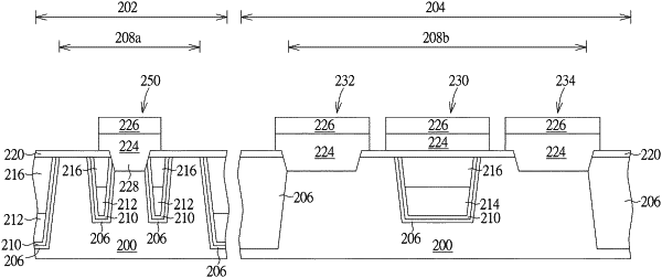
a substrate comprising a memory cell region and a peripheral circuit region defined thereon;
multiple active regions formed in the peripheral circuit region;
a buried gate structure formed in the active regions;
a conductive line structure formed right above the buried gate structure, wherein the conductive line structure completely overlaps the buried gate structure, and a longitudinal axis of the conductive line structure and a longitudinal axis of the buried gate structure extend in a same horizontal direction parallel to a surface of the substrate across the active regions, and an insulating layer is sandwiched between the buried gate structure and the conductive line structure, and the buried gate structure and the conductive line structure are physically spaced apart and electrically isolated from each other by the insulating layer; and
at least a bit line formed in the memory cell region, wherein a top surface of bit line in the memory cell region is leveled with a top surface of the conductive line structure in the peripheral circuit region.
|