| CPC H10B 12/053 (2023.02) [H10B 12/34 (2023.02)] | 18 Claims |
|
1. A manufacturing method of a semiconductor device, comprising:
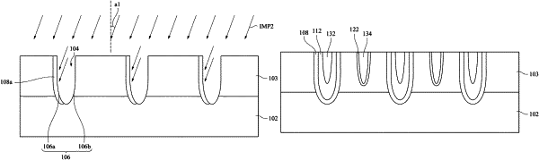
forming an opening in a substrate;
implanting a dopant in the substrate from a sidewall of the opening such that a doping region is formed in the substrate at the sidewall of the opening, wherein implanting the dopant in the substrate from the sidewall of the opening comprises implanting the dopant at a bottom portion of the opening;
after implanting the dopant in the substrate from the sidewall of the opening, filling a dielectric material in the opening to form a first dielectric structure; and
forming a passing word line in the first dielectric structure.
|