| CPC H10B 12/0335 (2023.02) [H01L 21/311 (2013.01); H01L 28/40 (2013.01); H01L 28/90 (2013.01); H01L 28/92 (2013.01); H10B 12/03 (2023.02); H10B 12/033 (2023.02); H10B 12/31 (2023.02)] | 4 Claims |
|
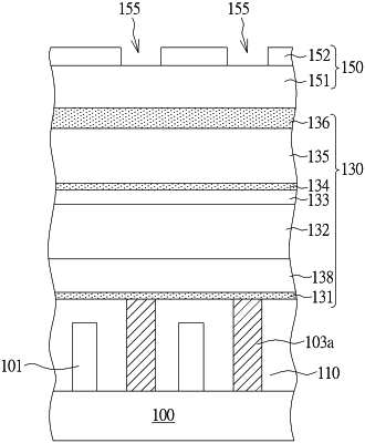
1. A semiconductor memory device, comprising:
a substrate;
a plurality plugs disposed in the substrate;
a stacked structure disposed on the substrate, the stacked structure comprising at least one oxide material layer and at least one nitride material layer stacked alternately on the substrate, and a first silicon containing layer and a second silicon containing layer stacked sequentially between the at least one oxide layer and the substrate;
a plurality of openings, disposed in the stacked structure to exposed each of the plugs respectively;
a plurality of expanding portions disposed at bottoms of the openings, wherein each of the expanding portions is in connection with each of the openings, a vertical sidewall of each of the expanding portions simultaneously contacts vertical sidewalls of the first silicon containing layer and the second silicon containing layer, and a bottommost surface of each of the expanding portions is coplanar with a topmost surface of each of the plugs, wherein the second silicon containing layer is silicon or amorphous silicon, an etching selectivity of the second silicon containing layer relative to that of the nitride material layer and the oxide material layer is 1:1:10; and
an electrode layer, disposed on surfaces of the openings and the expanding portions.
|