| CPC H05K 1/0393 (2013.01) [G02B 13/0085 (2013.01); H01L 27/14627 (2013.01); H10K 77/111 (2023.02); H10K 85/111 (2023.02); H05K 1/189 (2013.01); H10K 2102/311 (2023.02)] | 15 Claims |
|
1. A method comprising:
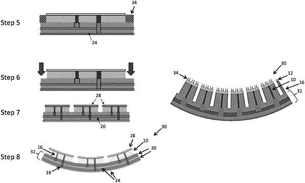
fabricating a wafer-based circuit including a plurality of circuit elements distributed across top surfaces of a plurality of spatially-separated wafer segments;
fabricating one or more through-silicon vias to electrically connect at least some of the plurality of circuit elements to interconnect points on a bottom surface of the wafer;
fabricating metal pillars on at least some of the interconnect points to extend these contacts vertically from the bottom surface of the wafer;
applying a polymer layer to the bottom surface of the wafer to form a backplane;
patterning an interconnect layer on top of the polymer layer, wherein the interconnect layer provides electrical connections between at least some of the metal pillars;
segmenting the wafer into a plurality of spatially-separated wafer segments, wherein at least one of spacings between the plurality of wafer segments or orientations of the plurality of wafer segments is adjustable by at least one of stretching or flexing the backplane.
|