| CPC H05K 1/0216 (2013.01) [H05K 1/0242 (2013.01); H05K 1/111 (2013.01); H05K 1/115 (2013.01); H05K 1/181 (2013.01); H05K 2201/0715 (2013.01); H05K 2201/10037 (2013.01)] | 20 Claims |
|
1. An electronic device comprising:
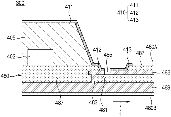
a board comprising a first conductive line, a second conductive line spaced apart from the first conductive line, a ground plane, and a conductive via hole electrically connecting the first conductive line and the ground plane;
at least one electronic component disposed on a first surface of the board and configured to at least partially overlap the ground plane;
an insulation member covering the at least one electronic component; and
a conductive layer,
wherein the conductive layer comprises:
a first part disposed on a surface of the insulation member,
a second part disposed on the first surface of the board and configured to extend from at least a portion of an edge of the first part in a direction away from the insulation member, and electrically connected to the first conductive line, and
a third part spaced apart from the second part, the third part extending from the first surface of the board in the direction away from the insulation member, and being electrically connected to the second conductive line,
wherein the first conductive line and the second part of the conductive layer are spaced apart from the second conductive line and the third part of the conductive layer with an opening in the board being interposed therebetween, and
wherein the electronic device comprises at least one transmission line comprising the second conductive line and the third part of the conductive layer and configured to transmit an electrical signal.
|