| CPC H04Q 11/0005 (2013.01) [H04J 14/0267 (2013.01); H04Q 11/0003 (2013.01); H04Q 2011/002 (2013.01); H04Q 2011/005 (2013.01); H04Q 2011/0073 (2013.01); H04Q 2213/31 (2013.01)] | 30 Claims |
|
1. An optical switch comprising:
a scheduler; and
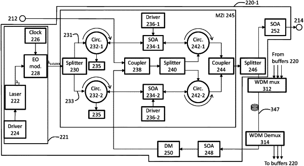
a buffer for buffering an optical packet including, arranged in a circuit, a clock generator for generating a clock signal, an optical unbalanced Mach Zehnder Interferometer (MZI) and a fiber delay line (FDL) having an FDL length,
wherein the optical packet has an optical packet signal,
wherein the scheduler is configured to insert the optical packet into the buffer and to determine a number of circulations of the optical packet through the circuit,
wherein the MZI modulates the clock signal based on the optical packet signal to create a reshaped optical packet after each circulation of the optical packet through the circuit, and
wherein the FDL introduces a delay in the optical packet proportional to the FDL length.
|