| CPC H04N 25/772 (2023.01) [H04N 25/531 (2023.01); H04N 25/58 (2023.01); H04N 25/616 (2023.01); H04N 25/771 (2023.01); H04N 25/79 (2023.01)] | 16 Claims |
|
1. An image sensor provided as an integrated circuit, the image sensor comprising a first substrate, a second substrate, vertically stacked and electrically interconnected with the first substrate, and a pixel array disposed within the first substrate, the pixel array comprising a plurality of pixels logically organized in pixel rows and pixel columns, wherein the pixel array is organized into a plurality of pixel subarrays and each pixel of the pixel array comprises:
a photoelectric element for integrating a photocharge while exposed to light during each one of a plurality of subframe exposures comprised in a frame interval;
a transfer gate for transferring at least a fraction of the integrated photocharge present in the photoelectric element at the end of each subframe exposure to a buffered charge-voltage converter;
the buffered charge-voltage converter for receiving and converting the transferred photocharge to a signal voltage, the buffered charge-voltage converter comprising a first charge accumulation element operatively connectable to at least one second charge accumulation element through a gain switch, to switch a conversion gain of the pixel between a high conversion gain and a low conversion gain, said at least one second charge accumulation element being provided in the first substrate or in the second substrate;
control circuitry adapted to trigger a partial or a complete transfer of said integrated photocharge in the photoelectric elements of each pixel row, by adjusting the amplitude of a transfer pulse applied to the transfer gate; and
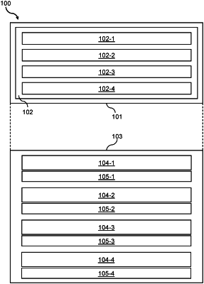
readout circuitry arranged on the second substrate, said readout circuitry comprising a plurality of parallelly operable readout block, each readout block being associated with a respective one of the plurality of pixel subarrays and configured to sequentially read out pixel row data of the respective pixel subarray at the end of each subframe exposure;
wherein the control circuitry, in at least one operating mode of the image sensor, is configured to:
trigger the partial transfer for all but the last one of the plurality of subframe exposures and the complete transfer for the last one of the plurality of subframe exposures,
time-interleave at least two rolling shutter control sequences associated with at least two time-overlapping subframes exposures of the plurality of subframe exposures in respect of each pixel subarray, and
control the gain switches (202-3) in each pixel row to operate the pixels at the low conversion gain for all but the last one of the plurality of subframe exposures and, for the last one of the plurality of subframe exposures, first operate the pixels at the high conversion gain and subsequently at the low conversion gain, and
wherein each readout block of the readout circuitry comprises, in a pipelined architecture:
an A/D conversion unit for sampling and digitizing pixel row data of the corresponding pixel subarray,
pixel memory logic conditionally combining digitized pixel row data with previously digitized pixel row data buffered in a pixel memory unit, and
the pixel memory unit for buffering digitized pixel row data output by the pixel memory logic.
|