| CPC H04N 25/772 (2023.01) [H04N 23/10 (2023.01)] | 8 Claims |
|
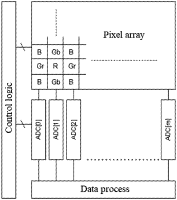
1. A pixel processing circuit configured for being applied to an image sensor of a bilateral parallel ADC readout architecture, the pixel processing circuit comprising:
a pixel array comprising a plurality of pixel units arranged in a Bayer array,
an Analog-to-Digital Converter (ADC) module comprising a plurality of analog-to-digital converters, and
a plurality of switch selection modules;
wherein a number of the switch selection modules is set to be half of a number of the analog-to-digital converters;
the plurality of analog-to-digital converters comprise first analog-to-digital converters located on a first side of the pixel array and second analog-to-digital converters located on a second side of the pixel array opposite to the first side;
each of the switch selection modules is configured to have a first unit disposed between the first side of the pixel array and one of the first analog-to-digital converters, and a second unit disposed between the second side of the pixel array and one of second analog-to-digital converters;
wherein the switch selection modules are configured to switch a communication between the pixel units and the first and second analog-to-digital converters on the opposite first and second sides of the pixel array, such that signals of green pixel units are read by the first analog-to-digital converters, and signals of remaining color pixel units are read by the second analog-to-digital converters,
wherein each of the switch selection modules comprises a plurality of switching circuits at least comprising a first switching circuit, a second switching circuit, a third switching circuit and a fourth switching circuit wherein a number of columns of the pixel array is even, the first switching circuit and the second switch circuit are located at the first side of the pixel array and the third switching circuit and the fourth switching circuit are located at the second side of the pixel array;
the pixel units in each of odd-numbered columns of the pixel array are respectively electrically connected to a first end of the first switching circuit of the switch selection module, and the pixel units in each of odd-numbered columns of the pixel array are respectively electrically connected to a first end of the third switching circuit of the switch selection module;
the pixel units in each of even-numbered columns of the pixel array are respectively electrically connected to a first end of the second switching circuit of the switch selection module, and the pixel units in each of even-numbered columns of the pixel array are respectively electrically connected to a first end of the fourth switching circuit of the switch selection module;
wherein second ends of adjacent first switching circuit and second switching circuit are electrically connected to a common first analog-to-digital converter, second ends of the adjacent third switching circuit and fourth switching circuit are electrically connected to a common second analog-to-digital converter, and each of the first switching circuit, the second switching circuit, the third switching circuit and the fourth switching circuit is electrically connected to only one analog-to-digital converter.
|