| CPC H04N 25/77 (2023.01) [H01L 27/14616 (2013.01); H04N 25/46 (2023.01); H04N 25/79 (2023.01); H01L 29/7869 (2013.01)] | 11 Claims |
|
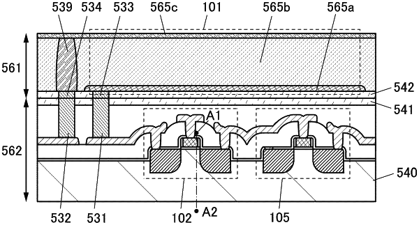
1. An imaging device comprising a pixel block, a first circuit, and a second circuit,
wherein the pixel block comprises a plurality of pixels arranged in a matrix,
wherein the plurality of pixels are electrically connected to the second circuit,
wherein the first circuit has a function of selecting pixels arranged in one row of the plurality of pixels,
wherein the first circuit has a function of selecting pixels arranged in a plurality of consecutive rows of the plurality of pixels,
wherein the first circuit has a function of changing the number of rows to be selected,
wherein the pixel has a function of generating first data,
wherein the pixel has a function of generating second data by adding a predetermined potential to the first data,
wherein the second circuit has a function of generating third data corresponding to a sum of the first data generated by the plurality of pixels,
wherein the second circuit generates fourth data by adding, to the third data, a potential corresponding to a sum of the second data generated by the plurality of pixels
wherein the first circuit is a shift register circuit comprising a first logic circuit, a second logic circuit, a twelfth transistor, a thirteenth transistor, a fourteenth transistor, and a fifteenth transistor,
wherein an output terminal of the first logic circuit is electrically connected to one of a source and a drain of the twelfth transistor,
wherein an output terminal of the second logic circuit is electrically connected to one of a source and a drain of the thirteenth transistor,
wherein the other of the source and the drain of the twelfth transistor is electrically connected to one of a source and a drain of the fourteenth transistor,
wherein the other of the source and the drain of the fourteenth transistor is electrically connected to the other of the source and the drain of the thirteenth transistor,
wherein the other of the source and the drain of the twelfth transistor is electrically connected to one of a source and a drain of the fifteenth transistor, and
wherein the other of the source and the drain of the fifteenth transistor is electrically connected to a power supply line.
|