| CPC H04N 23/80 (2023.01) [G11C 11/413 (2013.01)] | 4 Claims |
|
1. An image processing device comprising:
a circuit block in which an operation period is predetermined and intermittent operation is performed according to the operation period;
a plurality of SRAMs; and
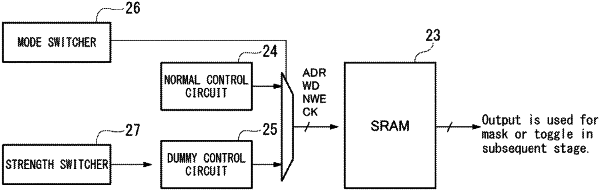
a dummy control circuit configured to increase an intensity of a dummy operation of an unused SRAM among the plurality of SRAMs for a certain period of time before the operation period of the circuit block, and to decrease the intensity of the dummy operation of the unused SRAM among the plurality of SRAMs for a certain period of time after the operation period of the circuit block.
|