| CPC H04N 23/741 (2023.01) [G01S 7/4863 (2013.01); G01S 17/89 (2013.01); G06T 7/521 (2017.01); H04N 23/56 (2023.01); G06T 2207/10028 (2013.01); G06T 2207/20208 (2013.01); G06T 2207/20212 (2013.01)] | 20 Claims |
|
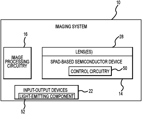
1. An imaging system comprising:
a semiconductor device comprising a plurality of single-photon avalanche diodes; and
control circuitry configured to:
set a bias voltage for the plurality of single-photon avalanche diodes to a first voltage level during a first sub-exposure;
expose the plurality of single-photon avalanche diodes to light pulses during the first sub-exposure;
set the bias voltage for the plurality of single-photon avalanche diodes to a second voltage level during a second sub-exposure, wherein the second voltage level is different than the first voltage level; and
expose the plurality of single-photon avalanche diodes to additional light pulses during the second sub-exposure; and
image processing circuitry configured to generate a depth map based on data from the first and second sub-exposures.
|