US 11,943,527 B2
Image capturing and display apparatus and wearable device
Yosuke Nishide, Kawasaki (JP); Yu Maehashi, Yokohama (JP); Masahiro Kobayashi, Tokyo (JP); Katsuyuki Hoshino, Kawasaki (JP); Akira Okita, Yamato (JP); and Takeshi Ichikawa, Hachioji (JP)
Assigned to Canon Kabushiki Kaisha, Tokyo (JP)
Filed by CANON KABUSHIKI KAISHA, Tokyo (JP)
Filed on May 3, 2023, as Appl. No. 18/311,297.
Application 18/311,297 is a continuation of application No. 17/330,578, filed on May 26, 2021, granted, now 11,706,518.
Application 17/330,578 is a continuation of application No. 16/365,952, filed on Mar. 27, 2019, granted, now 11,057,551, issued on Jul. 6, 2021.
Application 16/365,952 is a continuation of application No. PCT/JP2017/028860, filed on Aug. 9, 2017.
Claims priority of application No. 2016-199410 (JP), filed on Oct. 7, 2016.
Prior Publication US 2023/0269457 A1, Aug. 24, 2023
Int. Cl. H04N 23/57 (2023.01); G06F 1/16 (2006.01); G09F 9/30 (2006.01); H01L 27/14 (2006.01); H01L 27/144 (2006.01); H01L 27/146 (2006.01); H01L 27/15 (2006.01); H01L 31/02 (2006.01); H01L 31/0216 (2014.01); H01L 31/10 (2006.01); H01L 31/147 (2006.01); H04N 23/56 (2023.01); H04N 25/70 (2023.01); H05B 33/02 (2006.01); H05B 33/12 (2006.01); H05B 33/14 (2006.01); H10K 50/00 (2023.01); H10K 59/00 (2023.01)
CPC H04N 23/57 (2023.01) [G06F 1/163 (2013.01); G09F 9/30 (2013.01); H01L 27/14 (2013.01); H01L 27/144 (2013.01); H01L 27/146 (2013.01); H01L 27/15 (2013.01); H01L 31/02019 (2013.01); H01L 31/02164 (2013.01); H01L 31/10 (2013.01); H01L 31/147 (2013.01); H04N 23/56 (2023.01); H04N 25/70 (2023.01); H05B 33/02 (2013.01); H05B 33/12 (2013.01); H05B 33/14 (2013.01); H10K 50/00 (2023.02); H10K 59/00 (2023.02)] 20 Claims
OG exemplary drawing
 
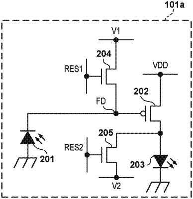
1. An apparatus comprising:
a photoelectric conversion element including a first impurity region in a silicon layer;
a light-emitting element for emitting light; and
a first transistor for resetting the light-emitting element, the first transistor including a second impurity region in the silicon layer and being arranged between the light-emitting element and the silicon layer.