| CPC H04N 23/55 (2023.01) [H01L 27/14618 (2013.01); H01L 27/14625 (2013.01); H01L 27/14636 (2013.01); H04N 23/54 (2023.01)] | 20 Claims |
|
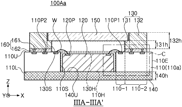
1. An image sensor device, comprising:
an image sensor;
a substrate including
an upper surface and a lower surface opposite to each other,
one or more inner surfaces at least partially defining a cavity extending through the substrate in a vertical direction that extends perpendicular to the upper surface which surrounds the cavity, wherein the image sensor is at least partially within the cavity, and
first and second pads isolated from direct contact with each other in a horizontal direction extending parallel to the upper surface, the first and second pads being on the upper surface;
an optical filter on both the upper surface of the substrate and the image sensor;
a first support member between the substrate and the optical filter, the optical filter being in direct contact with the first support member;
a second support member adjacent to the first support member on the substrate and closer to an outer edge of the substrate than the first support member in the horizontal direction; and
an optical device overlapping the optical filter and the image sensor in the vertical direction,
wherein the image sensor is electrically connected to the first pad,
wherein at least one of the first or second support members is electrically connected to the second pad, and
wherein the optical filter vertically overlaps the support member and the upper surface of the substrate.
|