US 11,943,032 B2
Method of signal generation and signal generating device
Yutaka Murakami, Kanagawa (JP); Tomohiro Kimura, Osaka (JP); and Mikihiro Ouchi, Osaka (JP)
Assigned to SUN PATENT TRUST, New York, NY (US)
Filed by Sun Patent Trust, New York, NY (US)
Filed on Jan. 27, 2023, as Appl. No. 18/102,338.
Application 18/102,338 is a continuation of application No. 17/551,984, filed on Dec. 15, 2021, abandoned.
Application 17/551,984 is a continuation of application No. 17/338,092, filed on Jun. 3, 2021, granted, now 11,240,084, issued on Feb. 1, 2022.
Application 17/338,092 is a continuation of application No. 16/582,644, filed on Sep. 25, 2019, granted, now 11,063,805, issued on Jul. 13, 2021.
Application 16/582,644 is a continuation of application No. 16/239,145, filed on Jan. 3, 2019, granted, now 10,476,720, issued on Nov. 12, 2019.
Application 16/239,145 is a continuation of application No. 15/987,016, filed on May 23, 2018, granted, now 10,225,123, issued on Mar. 5, 2019.
Application 15/987,016 is a continuation of application No. 15/496,406, filed on Apr. 25, 2017, granted, now 10,009,207, issued on Jun. 26, 2018.
Application 15/496,406 is a continuation of application No. 14/501,780, filed on Sep. 30, 2014, granted, now 9,667,333, issued on May 30, 2017.
Application 14/501,780 is a continuation of application No. 13/811,064, granted, now 8,885,596, issued on Nov. 11, 2014, previously published as PCT/JP2012/000352, filed on Jan. 20, 2012.
Claims priority of application No. 2011-033771 (JP), filed on Feb. 18, 2011; application No. 2011-051842 (JP), filed on Mar. 9, 2011; application No. 2011-093544 (JP), filed on Apr. 19, 2011; and application No. 2011-102101 (JP), filed on Apr. 28, 2011.
Prior Publication US 2023/0179280 A1, Jun. 8, 2023
Int. Cl. H04B 7/06 (2006.01); H04B 7/08 (2006.01); H04L 1/00 (2006.01); H04L 5/00 (2006.01); H04L 5/12 (2006.01); H04L 27/20 (2006.01); H04L 27/26 (2006.01); H04L 27/36 (2006.01)
CPC H04B 7/0667 (2013.01) [H04B 7/0682 (2013.01); H04B 7/0697 (2013.01); H04B 7/0842 (2013.01); H04L 1/0048 (2013.01); H04L 1/0071 (2013.01); H04L 5/0023 (2013.01); H04L 5/0082 (2013.01); H04L 5/12 (2013.01); H04L 27/20 (2013.01); H04L 27/2634 (2013.01); H04L 27/26524 (2021.01); H04L 27/368 (2013.01)] 2 Claims
OG exemplary drawing
 
1. A mobile terminal comprising:
a wireless communication circuit; and
a processor configured to switch between a first communication mode and a second communication mode, wherein
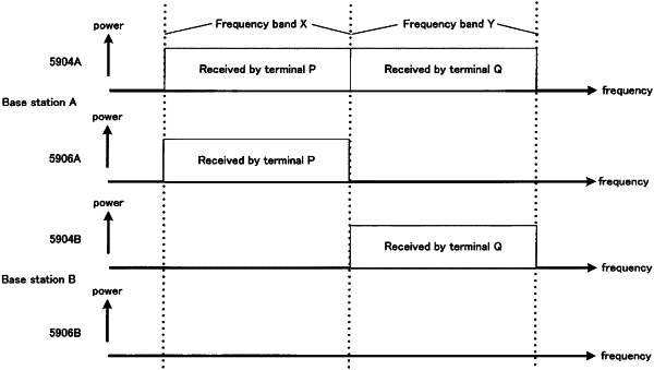
in the first communication mode, the wireless communication circuit receives first data and second data from a first base station and a second base station in a first frequency band and a second frequency band, respectively, at an identical time, the first data being identical to the second data, and the first frequency band being identical to the second frequency band, and
in the second communication mode, the wireless communication circuit receives third data from the first base station in a third frequency band or the wireless communication circuit receives fourth data from the second base station in a fourth frequency band, the third data being different from the fourth data, and the third frequency band being different from the fourth frequency band.