| CPC H04B 1/006 (2013.01) [G05F 3/16 (2013.01); H02M 1/0041 (2021.05); H02M 3/07 (2013.01); H03K 3/0315 (2013.01); H04B 1/44 (2013.01)] | 20 Claims |
|
1. A mobile device comprising:
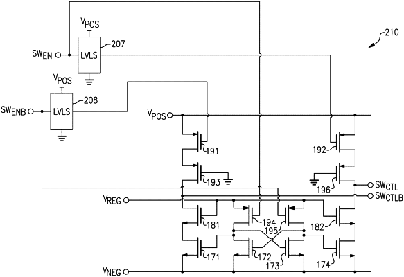
a power management system including a positive charge pump configured to generate a positive charge pump voltage, a negative charge pump configured to generate a negative charge pump voltage, and a voltage regulator configured to generate a regulated voltage; and
a front end system including a radio frequency switch controlled by a first switch control signal, and a level shifter operable to level shift a first switch enable signal to generate the first switch control signal at a first output, the level shifter including a first level-shifting n-type transistor and a first cascode n-type transistor in series between the negative charge pump voltage and the first output, a first level-shifting p-type transistor and a first cascode p-type transistor in series between the positive charge pump voltage and the first output, and a second cascode p-type transistor between the regulated voltage and a gate of the first level-shifting n-type transistor and controlled by the first switch enable signal.
|