| CPC H03M 1/1014 (2013.01) [H03M 1/002 (2013.01)] | 20 Claims |
|
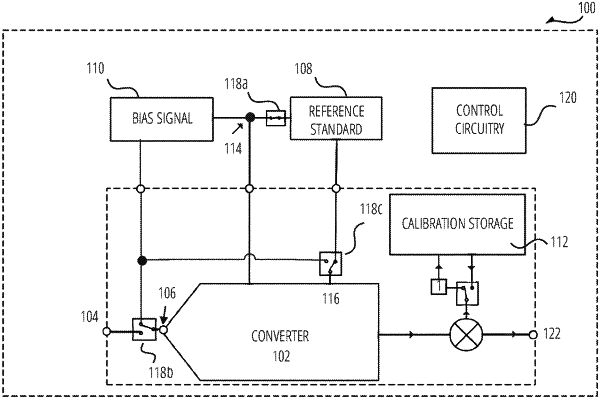
1. A system for processing an electrical signal, the system comprising:
analog-to-digital (ADC) signal converter circuitry including an ADC input node, an ADC output node, and an ADC reference node, the signal converter circuitry to receive an analog signal at the ADC input node and to generate, responsive to the analog signal and based on a signal received at the ADC reference node, a digital signal at the ADC output node;
bias signal circuitry to generate a reference bias;
reference standard circuitry to generate a reference standard signal; and
control circuitry to operate the system in a first mode and in a second mode, wherein:
in the first mode, the control circuitry is configured to couple the reference bias to the ADC input node and to couple the reference standard signal to the ADC reference node to generate a digital measurement of the reference bias using the reference standard signal as a reference at the ADC reference node; and
in the second mode, the control circuitry is configured to couple the analog signal to the ADC input node and the reference bias to the ADC reference node to generate a measurement of the analog signal using the reference bias as a reference at the ADC reference node.
|