| CPC H03M 1/0648 (2013.01) | 20 Claims |
|
1. A device, comprising:
an output node; and
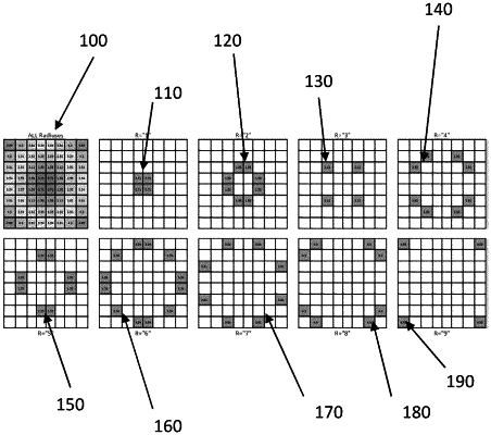
a plurality of electric components configured in an area of a substrate and coupled to the output node, wherein the device is configured to connect the electric components, in a pattern based on distances from the electric components to a center of the area, to reference voltages to produce a range of voltages at the output node, wherein the pattern reduces deviation from a linear output for a plurality of gradient directions of variabilities in the electric components in the area.
|