US 11,942,955 B2
Delay line, a delay locked loop circuit and a semiconductor apparatus using the delay line and the delay locked loop circuit
Yun Tack Han, Icheon-si (KR); and Kyeong Min Kim, Icheon-si (KR)
Assigned to SK hynix Inc., Icheon-si (KR)
Filed by SK hynix Inc., Icheon-si (KR)
Filed on May 31, 2023, as Appl. No. 18/326,671.
Application 18/326,671 is a division of application No. 17/347,312, filed on Jun. 14, 2021, granted, now 11,750,201.
Application 17/347,312 is a continuation in part of application No. 17/149,479, filed on Jan. 14, 2021, abandoned.
Application 17/149,479 is a continuation in part of application No. 16/911,888, filed on Jun. 25, 2020, granted, now 11,206,026, issued on Dec. 21, 2021.
Claims priority of application No. 10-2019-0110563 (KR), filed on Sep. 6, 2019; and application No. 10-2019-0110569 (KR), filed on Sep. 6, 2019.
Prior Publication US 2023/0308103 A1, Sep. 28, 2023
Int. Cl. H03L 7/081 (2006.01); H03K 5/134 (2014.01); H03L 7/087 (2006.01); H03L 7/089 (2006.01)
CPC H03L 7/0816 (2013.01) [H03K 5/134 (2014.07); H03L 7/0895 (2013.01); H03L 7/087 (2013.01)] 9 Claims
OG exemplary drawing
 
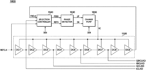
1. A delay locked loop circuit comprising:
a delay line configured to delay, based on a delay control voltage, a reference clock signal to generate an internal clock signal and a feedback clock signal;
a selection controller configured to provide the internal clock signal and the feedback clock signal respectively as a first selection clock signal and a second selection clock signal when a deterioration enable signal is disabled, and to provide the reference clock signal as the first selection clock signal and the second selection clock signal when the deterioration enable signal is enabled;
a phase detector configured to compare phases of the first selection clock signal and the second selection clock signal to generate an up-signal and a down-signal; and
a charge pump configured to generate the delay control voltage based on the up-signal and the down-signal.